For my Master’s thesis at EPFL, I implemented a System-on-Chip (SoC) for an FPGA in Verilog, centred around the Hazard31 RISC-V processor. The system is designed as an educational platform that enables EPFL students to gain practical experience in both software development and hardware design for embedded systems.
The platform targets the Gecko5Education2 board, developed by Prof. Kluter. Since the Verilog source code is available to students and can be synthesised directly onto the FPGA, they are free to explore and modify the system architecture themselves. The SoC also provides an out-of-the-box debug interface, enabling remote software debugging.
Debugging hardware directly on the device, however, presents additional challenges. Building on work that began as a semester project, I continued the development of a custom Logic Analyser as part of my Master’s thesis. The Logic Analyser was implemented from scratch and consists of two main components.
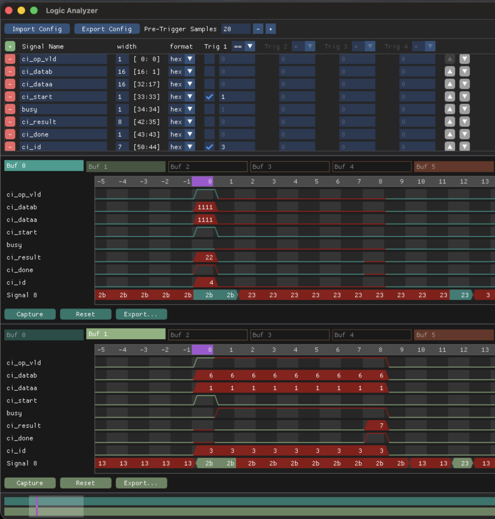
The first is a hardware component integrated directly into the SoC. It contains the core logic of the Logic Analyser and is memory-mapped to the system bus, allowing it to be accessed through the remote debugging protocol. The second component is a software application (shown in the screenshot below), which simplifies communication with the Logic Analyser and provides a visual representation of the recorded signals.
In the application, users can view a list of all signals connected to the Logic Analyser and upload a trigger configuration to the board. Once the specified trigger condition is met—that is, when the signals match the configured conditions—the Logic Analyser captures and stores the signal values for exactly 512 clock cycles.
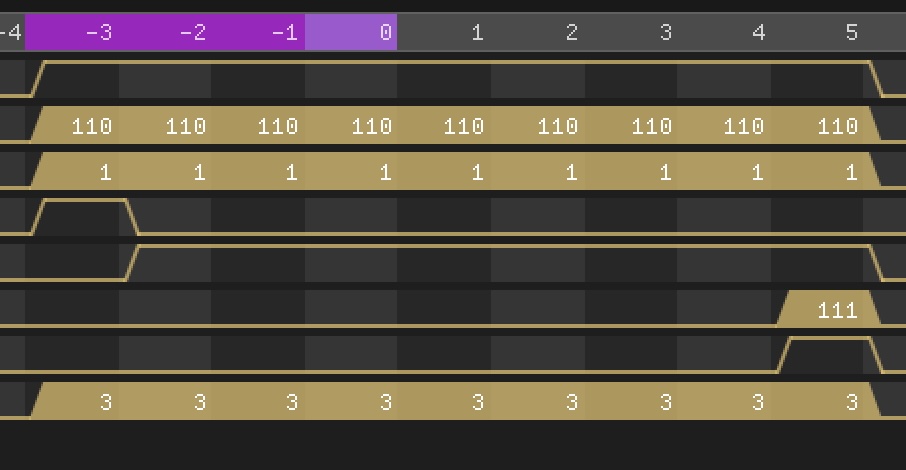
After the capture is complete, the desktop application downloads the recorded data and visualises the signals as waveforms in a diagram.
- Hazard3: https://github.com/wren6991/hazard3 ↩︎
- Gecko5Education: https://gecko5education.ti.bfh.ch/gecko5education/index.html ↩︎